This is the second in a series of posts documenting a project funded by an Entrepreneur-in-Residence Award from Creativeworks London. See an earlier post for the first design iteration.
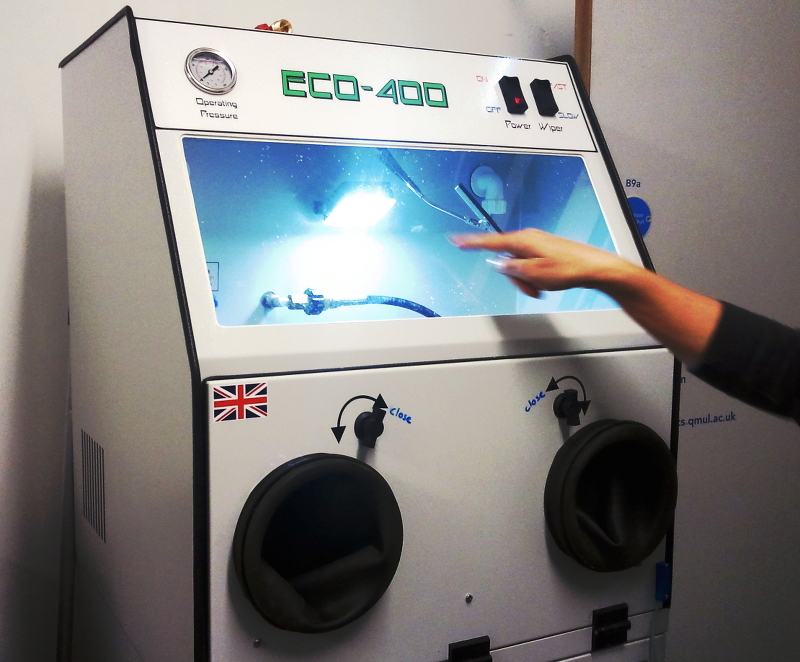
After working with the laser cutter and inkjet printer to bring some initial ideas to a physical form, I was ready to move on to the 3D printer. The Materials Processing Lab at Queen Mary has a Objet30 Prime which is printer that builds up a liquid layer of material that is then UV cured. It can print 16-28 microns per layer, depending the material being printed.
3D Printed Buttons
The biggest barrier to the 3D printer for me was learning how to create a model. I worked with AutoCAD and managed to learn enough from online tutorials to get what I wanted. I started by creating a solid cylinder, seen below in a hard white plastic, surrounded by a translucent material printed as a support structure.
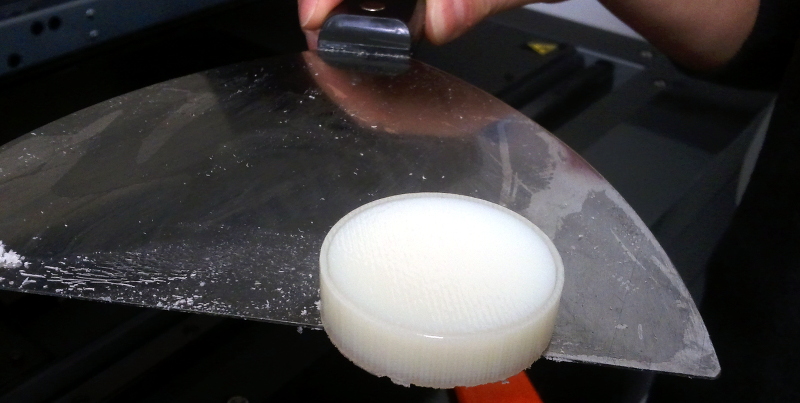
The support material is washed away in a power washing station. The station has a staggering number of significant design flaws, but its little automatic windshield wiper makes it endearing.
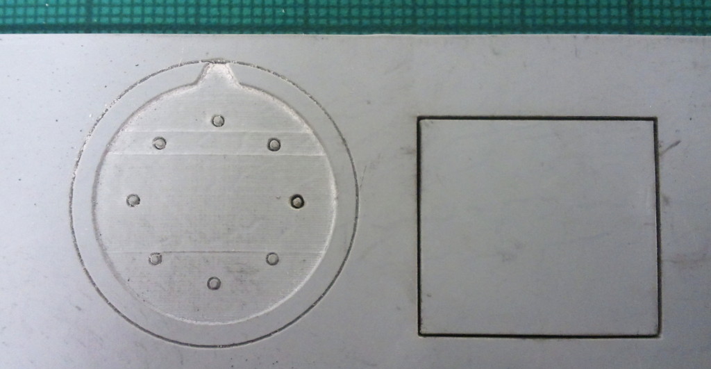
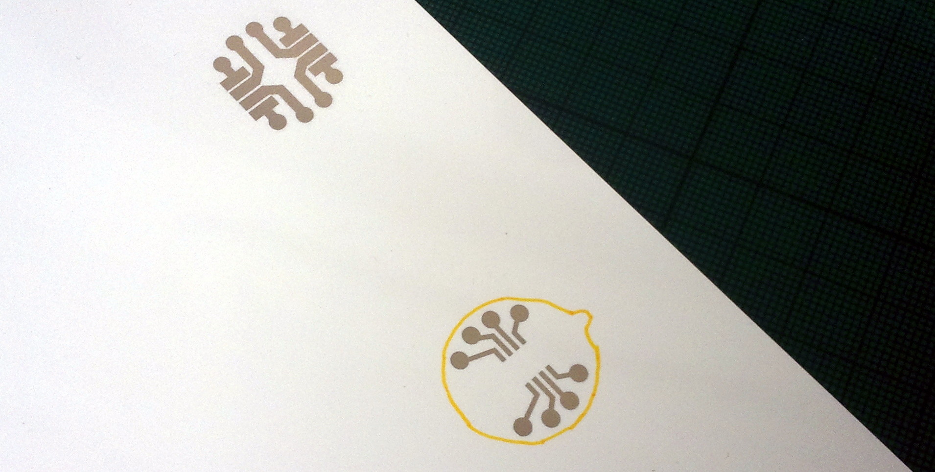
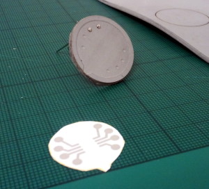
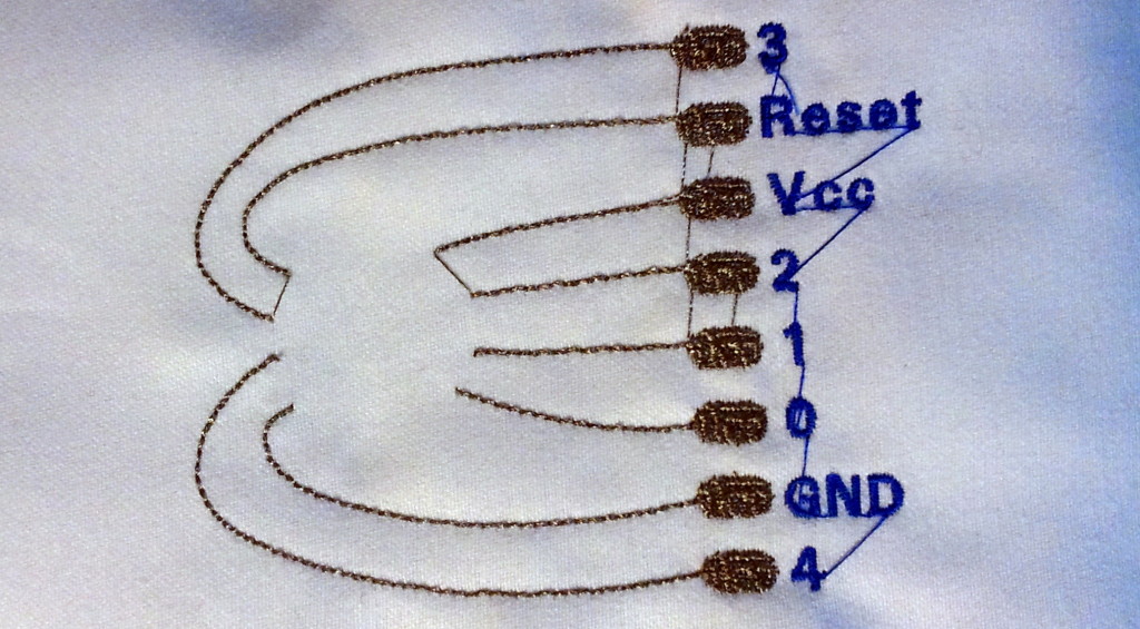
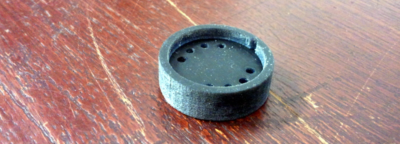
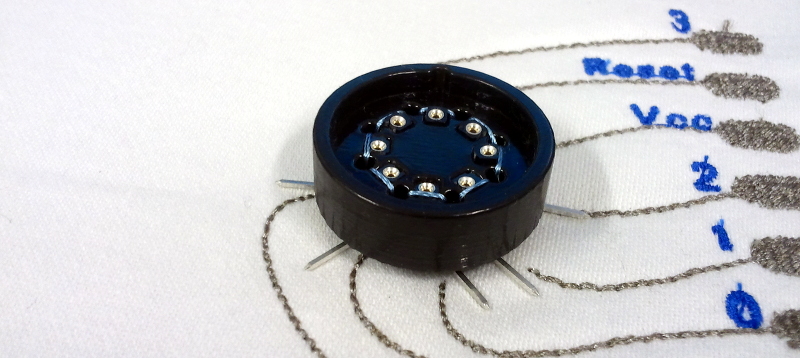
The initial printed design was a 3D interpretation of the laser cutter layout. Eight holes were printed in a cylinder with a recessed circle so that it could hold both a PCB and contacts to reach the pins. A notch was included to allow the inserted PCB to fit in only one way. This initial print can be seen below. It is created with Tangoblack FLX973, a flexible, rubber-like material. It was printed with a matte finish, an effect caused by being printed with the support material fully encasing the object.
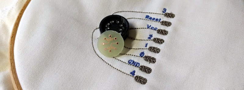
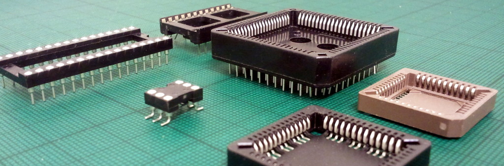
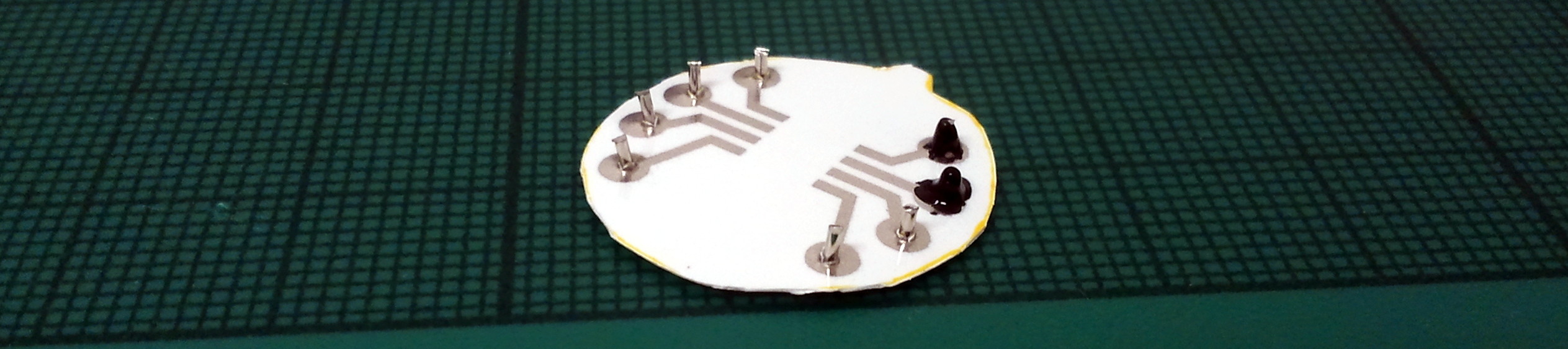
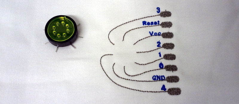
The first change made to the design was the position and size of the holes for the contacts. The first design iteration used sewing straight pins as contacts, which were handy for a very quick and dirty proof of concept, but certainly not ideal for anything more robust than that. After hunting through electronic component catalogues, I came across turned pin header sockets used for wire wrapping. The long legs of the sockets gave plenty of clearance to bend the legs out from under the button and reach the conductive thread of the embroidered circuit. The legs could then be hand-sewn with conductive thread.
The design change was to equally distribute the sockets around the PCB/button in a circle, as opposed to two arced groupings. This provided the maximum distance between the contacts and made it easier to create design files in multiple software packages for the different prototyping processes.
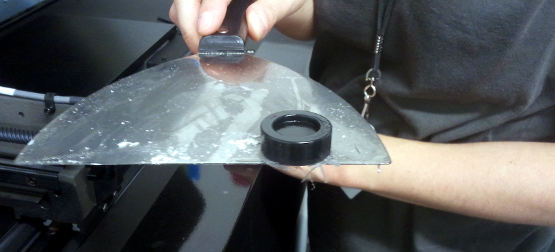
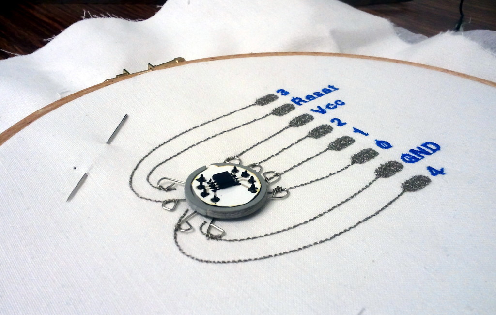
To work towards a functioning prototype, I laser cut acrylic to play the role of the PCB.
After discussing the prototype with Andrew, he pointed out that the button hole could cause too much mechanical strain on the socket legs. The stitching holding the legs in place was the only physical connections holding the button in place. To improve this, we added holes to allow the button to be stitched to the fabric directly. They were placed slightly outside the sockets so that the thread could provide a mechanical strain-relief for the socket legs.
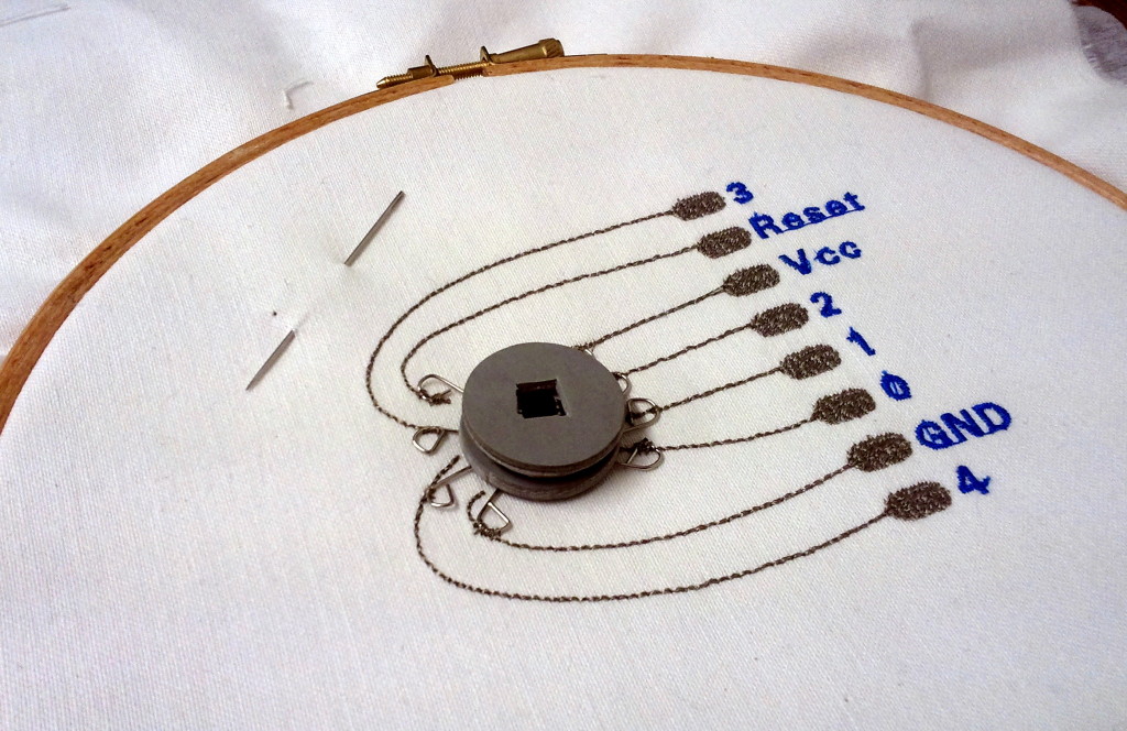
The print below uses the gloss effect in the same rubber-like plastic as the print in the photo above. The gloss effect is achieved by not surrounding the object in the support print material, but using it only where structurally necessary.
Milled PCB
It was then time to move on to the PCB prototype. I created the design in EAGLE – with assistance from Andrew as I am far from fluent with that software tool. The PCB was then milled on the LPKF S103 PCB Mill located in the Electronics Lab at Queen Mary. Below is a PCB as it came off the milling bed on the right and after some sanding on the left.
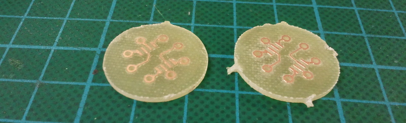
The PCB fit cleanly into the 3D printed button with all the holes lining up as they were supposed to. However, the inserting and removing the PCB and pins into the sockets highlighted a number of weaknesses in the design.
Reflections on Iteration 2
The printed material wasn’t adhered to the sockets in any way; the sockets were held in place only by the friction of the socket housing against the printed holes. The insertion and then removal of a pin into a socket caused the socket to pull away from the button.
The legs of the sockets were bent so the button could sit against the fabric, but they weren’t formed into a shape such as a loop. This meant that the force of removing a pin from the socket could cause the leg to be slid out of the stitching holding it in place.
Lastly, the 3D print material couldn’t withstand a shearing force where the rim that holds the PCB in place meets the main body of the button. The rim quickly fell apart, though anecdotally, the glossy finish seems to hold together better than the matte.
These concerns will be addressed, and hopefully improved upon, in the next and final design iteration of the project.