I’ve started referring to electronics connected to soft sensors and hidden on a PCB in a pocket of a garment as the “pocket of shame”. By no mean do I mean any shame on the designers and engineers who were forced to place their circuitry in a pocket, but that it’s a shame we haven’t found a better solution. Beautiful, tactile, and flexible, textile electronic sensors can be woven, knit, or stitched into clothing, but the circuitry needed to process the data generated by those sensors or to send that data off to be processed on another device, is still often mounted on rigid PCBs.
This past October I started a short research project funded by the Creativeworks London Entrepreneur-in-Residence Scheme at the School of Electronic Engineering and Computer Science at Queen Mary University of London. I’m exploring how PCBs can be better integrated into garments with soft sensors, not by trying to transform the PCBs into something flexible, but by hiding them in the already “hard” parts of a garment – buttons.
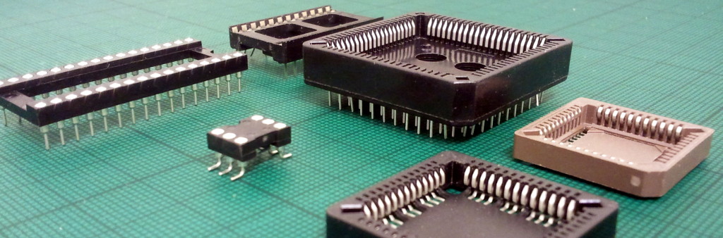
I’m working with Andrew McPherson, a Senior Lecturer at QM, and Berit Greinke, a PhD student and lab technician in the Materials Processing Lab. We are using the rapid prototyping facilities available in the School to create buttons that are inspired by the chip holder/adapters shown in the photo above. The idea is to create a housing that can be sewn to a garment (with both conductive and non-conductive threads) that remains in place whilst the PCB it houses can be removed.
The Housing
The first design iteration has been focused on a SOIC package of an ATtiny and using the tools with the smallest barriers of use, whether cost, bureaucracy or my own skillset.
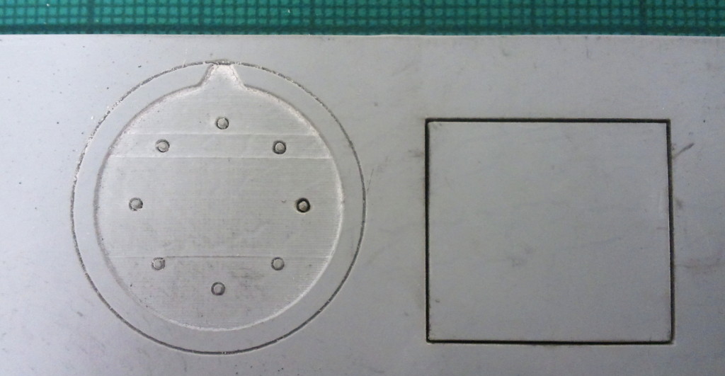
The housing has been developed using laser cut and etched rubber to make a recessed area for the PCB to sit in with 8 holes for pins to make contact with the PCB and fabric sensor.
The Circuit
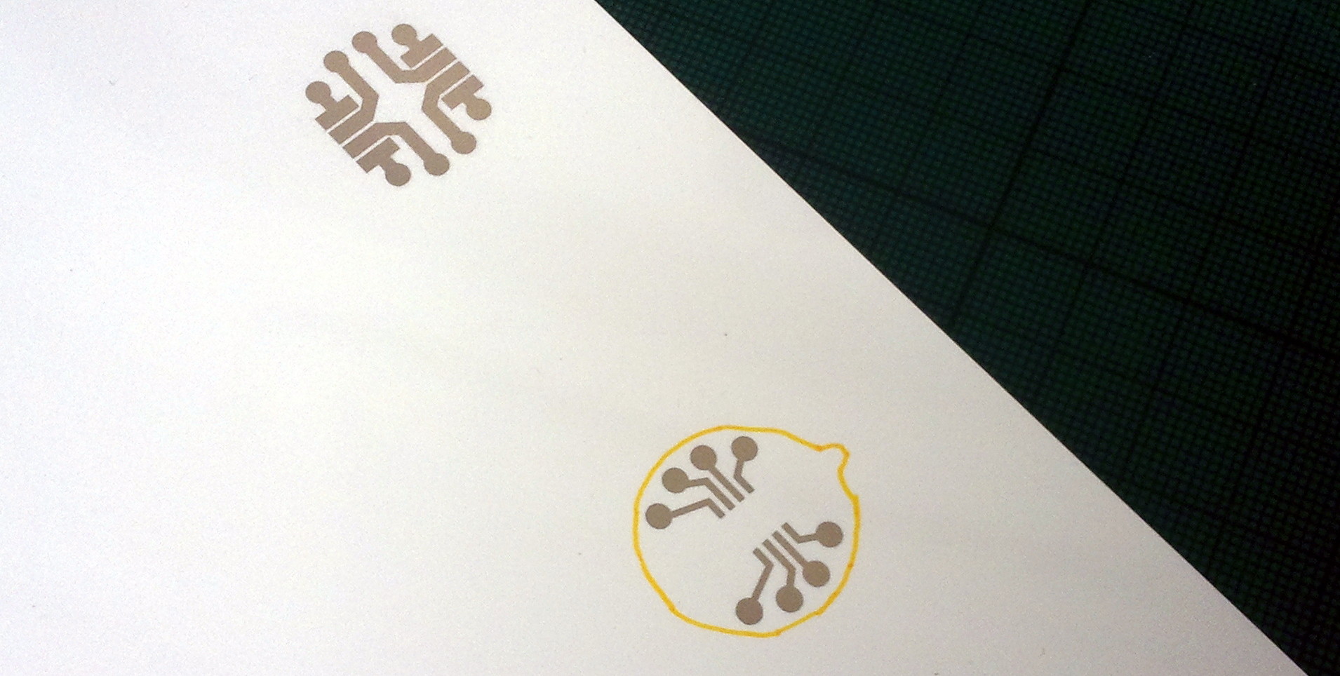
The circuit was printed on paper using a Brother DCP 145C and silver nano particle ink.
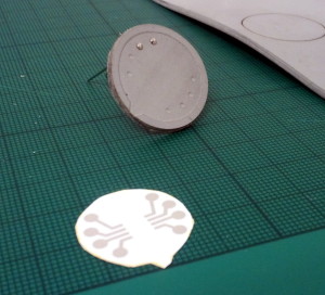
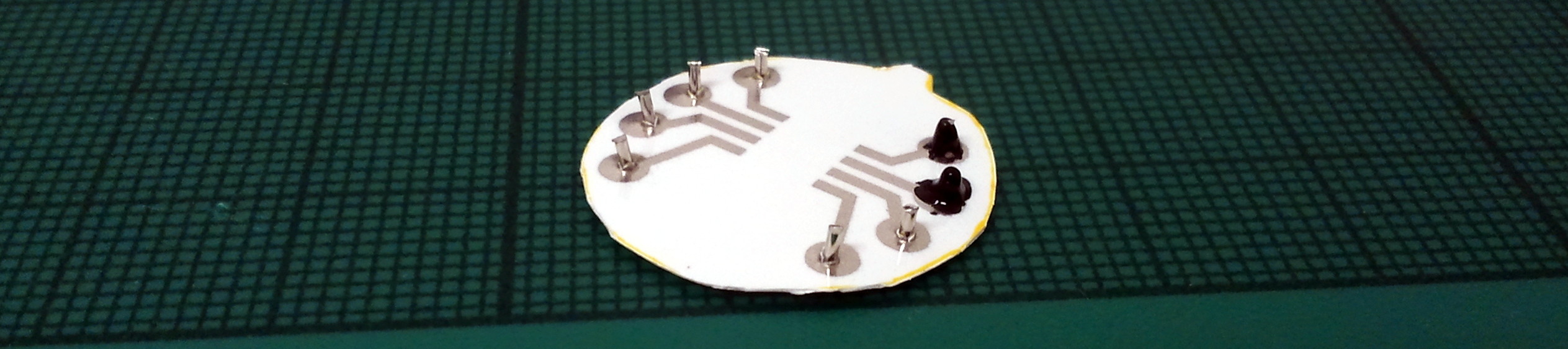
I used clipped sewing straight pins as the contacts as they have broader flat heads that sat against the underside of the paper. They pierced the paper and then were electrically connected to the printed circuit with Bare Conductive Electric Paint.
The Fabric Connection
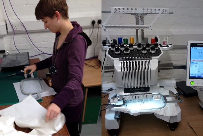
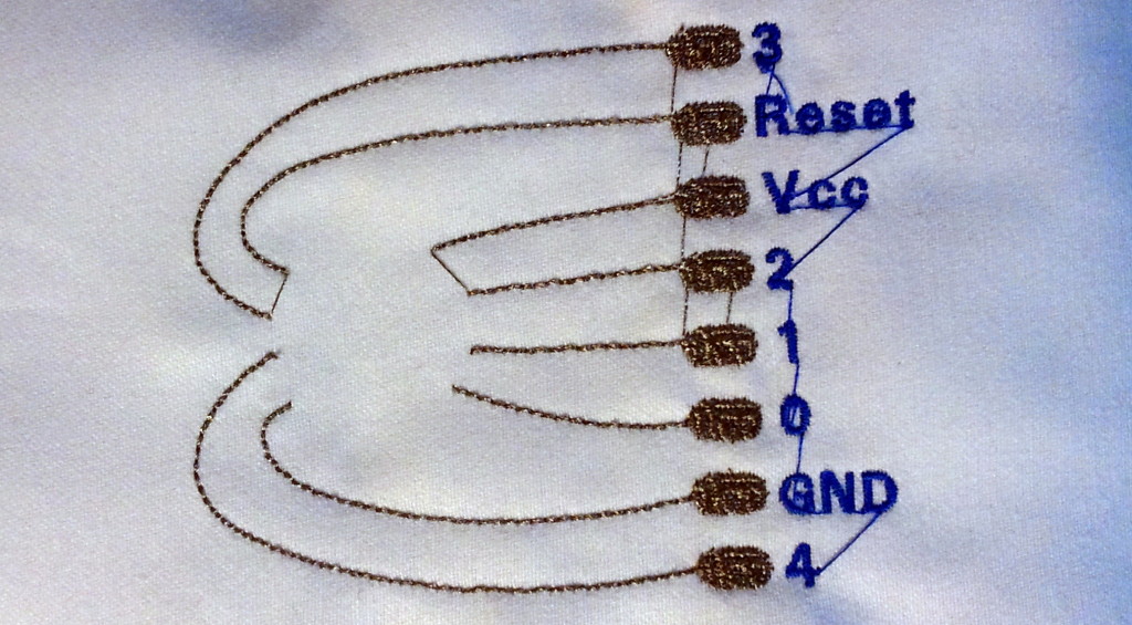
The remaining piece is the fabric circuit that the button interfaces with. With much training and assistance from Berit, I designed and embroidered a breakout circuit for the button to be sewn onto.
A Brother Pr1000e was used to embroider the circuit with Shieldex 110f 34dtex 2 ply yarn by Statex. It’s mostly done automatically, but some care needs to be taken to manually stop the machine’s thread cutter from trying to cut the conductive thread.
Here is the circuit when it comes off the machine, before trimming all the threads (which is something that can be programmed into the design for the machine to handle, but I hadn’t tackled that yet as this was my first time working with the software).
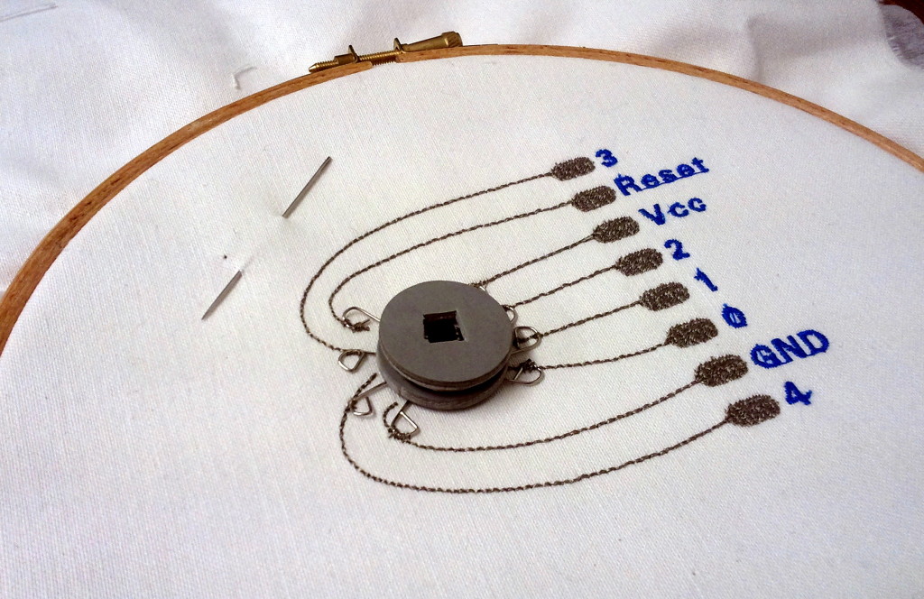
And here it is with the laser cut housing sewn in place. I used sewing straight pins to piece the rubber and then clipped the ends and formed them into loops.

The ATtiny was cold soldered into place on the circuit board with Bare Conductive Electric Paint and the circuit board placed in the holder.
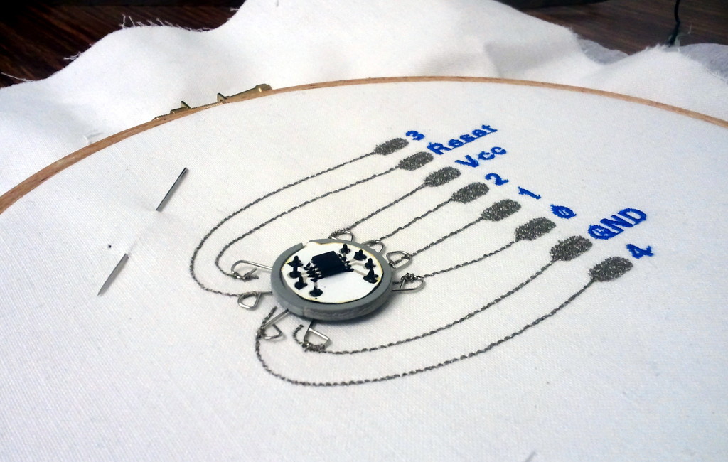
A second piece of rubber served as a means to hold the circuit board in place.
Reflections on Iteration 1
The prototype button is able to make an electrical connection ranging from 30 to 80 Ohms of resistance from the chip leg to the sewn breakout pad. However, it is not a stable connection, but rather fragile both due to the materials and how the “sandwich” of layers meet each other.
The ability to so quickly make physical prototypes was incredibly useful, even though they are certainly not the best materials and tools to be used for the final version. Now that a general form factor has been settled on, the next iteration will utilise the 3D printer instead of laser cutting and a milled PCB instead of a printed paper circuit board.
The use of straight pins as electrical contacts were convenient as they were readily available in the lab, but won’t be used in future iterations. Another solution needs to be sourced, probably by perusing electronics components catalogues.